The Impact of Pre-treatment in Solder Mask Bridge of PCB Production
Introduction:
In the PCB industry, in order to ensure the insulation of solder mask of the printed circuit boards, as well as prevent the oxidation of the PCB surface and beautify the appearance, it is usually necessary to apply a layer of solder mask on the PCB surface and the substrate that do not need to be soldered. With the rapid development of electronic industry, the solder mask technology has been developed rapidly.
The solder mask between the pads of SMD is called Solder Bridge, whose function is to prevent the bridging when soldering. With the increase of wiring density, the spacing of SMT soldering feet becomes smaller and the width of solder mask bridge decreases, which makes soldering pretreatment increasingly show its important status.
Test Method:
Take the same type of polished CCL, respectively with needle brush and non-woven cloth grinding, volcanic ash, sandblasting these kinds of pretreatment. The solder mask process was carried out after grinding the boards. Solder bridge test film was used for soldering exposure during alignment. PCB after development and curing was compared and tested according to different methods.
1) The tension test of 3M tape was carried out on the 0.05mm, 0.075mm, 0.1mm and 0.125mm solder bridges in PCBs manufactured with different pretreatment methods.
2) PCBs with different pretreatment methods were respectively treated with lead-free HASL, immersion gold, immersion tin and other surface treatments. The treated PCBs were subjected to a 3M tape tensile test and sliced to compare the degree of attack on the solder masks
Analysis in Test Results:
Figure 1 is the SEM diagram of copper layer after different pretreatment. It can be seen from the figure analysis that, for the board surface treated with needle brush and non-woven cloth pretreatment, since the surface of copper layer is roughened by brush wheel, the wear marks on the copper layer are all in one direction, and the apparent state of the copper layer is changed at the same time, so it has a certain repairing effect on the defects of the copper surface itself, but the copper surface is like a slight trench. The volcanic ash is used to spray volcanic ash abrasive onto the grinding roller to rough the surface, so the copper surface can be rough. Therefore, the adhesion between the solder mask and the copper layer can be improved and the loose oxide layer on the copper surface can be effectively removed. Sand blasting is a high pressure way to spray powder such as alumina directly on the copper surface, to reach the rough copper surface, so the contact area is large, copper surface binding force is good.

Analysis in Solder Mask Results:
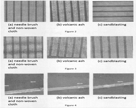
Figure 2 shows the effect of solder mask of polished CCL after different pretreatment and development. FIG. 3 is the effect of the solder bridge of CCL after soldering curing. FIG. 4 is a section diagram of the solder bridge after curing.

Analysis in Lead-free HASL Results:
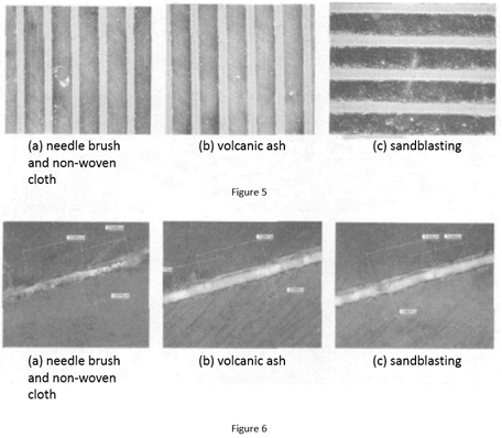
Figure 5 is a rendering after the lead-free HASL. Figure 6 is a section diagram of the solder bridge after the lead-free HASL.

Analysis in Immersion Gold:
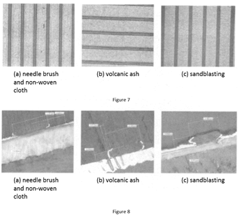
Figure 7 is the effect diagram of the PCB after immersion gold after soldering, and figure 8 is the section diagram of the soldering bridge after immersion gold.

Analysis in Immersion Tin:
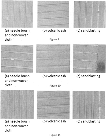
FIG. 9 is the solder bridge (0.075mm) diagram of the soldered PCB after immersion tin. FIG. 10 shows the tin soldering bridge (0.1mm) of the soldered PCB after immersion tin. FIG. 11 shows the soldering bridge (0.125mm) of the soldered PCB after immersion tin.

Conclusion:
For these three pretreatments, the copper surfaces of (b) volcanic ash and (c) sandblasting are uniformly rough. The copper surface of (a) needle brush and non-woven cloth is worn and slightly furrowed.
Through the above tests, it can be found that the PCB treated with volcanic ash has the smallest amount of solder mask be eroded on its surface, and when immersion tin, the solder bridge of 0.1 mm or more is not found to fall off. For PCB treated with needle brush and nonwoven fabric, the amount of solder mask erosion on the surface is much smaller than that of sandblasted PCB, and when immersion tin, the solder bridge of 0.125mm or more is not found to fall off. The solder mask on the surface of sandblasted PCB was the most eroded, and the soldering Bridges below 0.125mm were found to be peeling off when immersion tin was carried out.
That is to say, volcanic ash is best used as a pretreatment, followed by needle brush and non-woven cloth. Sandblasting has the worst effect as a pretreatment.
Comments
Post a Comment