Posts

Showing posts from June, 2020

Meet New Special PCB Technologies in PCBWay!

Image
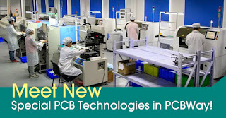
As a PCB innovation company, PCBWay is committed to solving the pain points of PCB procurement and meeting customers' various PCB procurement needs - offering special plates such as Rogers, copper substrates, aluminum substrates, and high-frequency high-speed HDI. Recently, with the efforts of the technical department, PCBWay has added many special technologies.   1 Impedance control The resistance encountered by high-frequency signals or electromagnetic waves in the transmission signal lines of electronic components is called characteristic impedance. When the digital signal is transmitted on the board, the characteristic impedance value of the PCB must match the electronic impedance of the head and tail components. Once there is a mismatch, the transmitted signal energy will be reflected, scattered, attenuated or delayed, seriously affecting signal integrity. In this case, impedance control must be performed to match the characteristic impedance value of the PCB to the co

What is PCB Tombstone?

Image
Introduction The tombstone phenomenon is that during welding process of the MLCC and PCB, one end of the MLCC leaves the welding area and is inclined or standing upright. The main reason is the unbalanced wetting force at both ends of the MLCC during the welding process. The main factors that produce unbalanced wetting force are: (1) Both ends of MLCC cannot be melted at the same time; (2) The pad design is unreasonable. According to the mechanical mechanism, it is proposed to keep the surface of the MLCC clean, pay attention to the reasonable pad design, avoid the weakening of the solder paste activity, and ensure that the MLCC melts at both ends. This measure can effectively prevent the tombstone phenomenon and has achieved good results in actual production. Before welding, the two ends of the chip Multi-layer Ceramic Capacitors (MLCC) are temporarily positioned with solder paste and board pads. When the welding is successfully completed, they become part of the assembled circuit boa

How to avoid the negative effects of vias in high-speed PCB design

Image
The basic concept of vias Via is an important part of multilayer PCB. The cost of drilling usually accounts for 30% to 40% of the cost of PCB. Simply put, each hole on the PCB can be called via. From a functional point of view, vias can be divided into two categories: one is used as an electrical connection between layers, the other is used for fixing or positioning devices. In terms of technology process, these vias are generally divided into three categories, namely blind vias, buried vias, and through-hole. The blind holes are located on the top and bottom surfaces of the printed circuit board and have a certain depth. They are used for the connection between the surface layer circuit and the inner layer circuit below. The depth of the hole usually does not exceed a certain ratio (aperture). Buried hole refers to the connection hole located in the inner layer of the printed circuit board, it will not extend to the surface of the circuit board. The above two types of holes are locate

ANAVI Fume Extractor—the smart open source solder absorber

Image
Soldering is quiet fun while the fumes during the soldering are harmful to our health. Thus, it’s a must to have a fume extractor. Now, the ANAVI Fume Extractor is a great choice for all the makers. “ANAVI Fume Extractor is a smart, open source, solder smoke absorber. It is powered by a Wi-Fi development board with an ESP8266, an 80 mm fan, and a replaceable filter. ANAVI Fume Extractor has dedicated slots for a mini OLED I²C display and an MQ-135 gas sensor module, as well as slots for up to three additional I²C sensor modules for measuring temperature, humidity, light, and barometric pressure. Furthermore, there are UART pins for easy flashing of custom firmware and an extra GPIO for connecting external peripherals. " ANAVI Fume Extractor is an entirely open source project which combines open source hardware and open source software. It is certified by the Open Source Hardware Association (OSHWA) with UID BG000060. ANAVI Fume Extractor can work with popular open source home auto

Quantum Leap: Any-layer HDI Technology of PCBWay

Image
Introduction PCBWay  is a high-end PCB R&D and manufacturing company. Since 2015, the company is keenly aware that the future demand for high-density interconnection boards and high-frequency high-speed boards in communications, medical, industrial control, and other industries will show explosive growth. So we further upgrade and adjustment of product strategy, accurate positioning on HDI high-density interconnect circuit boards, 5G communication high-frequency high-speed circuit boards. On the basis of the gradual and stable production of 1–5 order HDI boards in the past 4 years, the technical center has once again faced the difficulties, and successfully developed a 14-layer 6-stage any-layer HDI board. Overview of Any-layer HDI Board At present, China’s 5G communication technology has reached the world’s leading level, and 5G commercialization has been fully rolled out. The 5G communication circuit board is highly integrated and the PCB space cannot be increased, resulting in m

Types and Characteristics of Ceramic Substrates

Image
Ceramic substrate refers to a special process board where the copper foil is directly bonded to the surface (single side or double side) of alumina (Al2O3) or aluminum nitride (AlN) ceramic substrate at high temperature. Compared with traditional FR-4 or aluminum substrate, the ultra-thin composite substrate made has excellent electrical insulation performance, high thermal conductivity, excellent soft solderability, and high adhesion strength, and can be etched various graphics like the PCB, with great current carrying capacity. It is suitable for products with high heat generation (high-brightness LED, solar energy), and its excellent weather resistance is more suitable for harsh outdoor environments. What are the types of ceramic substrates? 1. According to the material 1). Al2O3 So far, the alumina substrate is the most commonly used substrate material in the electronics industry, because of its mechanical, thermal, and electrical properties compared to most other oxide ceramics, i